
Your Trusted Electronic
Manufacturing Services Parter

Your Trusted Electronic
Manufacturing Services Parter

Your Trusted Electronic
Manufacturing Services Parter
SCROLL
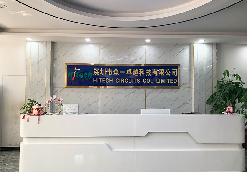
ABOUT HITECHPCBA
Hitech is China's leading electronic manufacturing services provider, we help you turn your ideas into reality, and providing PCB Design, PCB manufacturing, PCB assembly. Electroic parts sourcing, Assembly testing and One-Stop PCBA assembly services.
You can always count on us for high-quality and cost-effective electronics manufacturing services. Our services include: PCB design and layout, 1-48 layers precision PCB manufacturing, PCBA manufacturing, electronic components purchasing, PCB Soldering and Assembly, especially prototype and small batch orders. we have the advantages of a quick quote, fast production, fast delivery.
YOUR REQUIREMENT
A successful PCB layout will have its circuitry physically arranged for the best electronic performance of the board while also being fully manufacturable. This requires diligently managing library parts, CAD setups and parameters, component placement, trace routing, and the design of the power delivery network (PDN)
A successful PCB layout will have its circuitry physically arranged for the best electronic performance of the board while also being fully manufacturable. This requires diligently managing library parts, CAD setups and parameters, component placement, trace routing, and the design of the power delivery network (PDN)
A successful PCB layout will have its circuitry physically arranged for the best electronic performance of the board while also being fully manufacturable. This requires diligently managing library parts, CAD setups and parameters, component placement, trace routing, and the design of the power delivery network (PDN)
A successful PCB layout will have its circuitry physically arranged for the best electronic performance of the board while also being fully manufacturable. This requires diligently managing library parts, CAD setups and parameters, component placement, trace routing, and the design of the power delivery network (PDN)
A successful PCB layout will have its circuitry physically arranged for the best electronic performance of the board while also being fully manufacturable. This requires diligently managing library parts, CAD setups and parameters, component placement, trace routing, and the design of the power delivery network (PDN)
A successful PCB layout will have its circuitry physically arranged for the best electronic performance of the board while also being fully manufacturable. This requires diligently managing library parts, CAD setups and parameters, component placement, trace routing, and the design of the power delivery network (PDN)
A successful PCB layout will have its circuitry physically arranged for the best electronic performance of the board while also being fully manufacturable. This requires diligently managing library parts, CAD setups and parameters, component placement, trace routing, and the design of the power delivery network (PDN)
A successful PCB layout will have its circuitry physically arranged for the best electronic performance of the board while also being fully manufacturable. This requires diligently managing library parts, CAD setups and parameters, component placement, trace routing, and the design of the power delivery network (PDN)
WHY CHOOSE US?

8000+
Trusted by more than 10,000 Electronic Engineers
9000+
The maximum desian scale is90000pin
6000+
More Than 6,000 Electronic Contract
99%
99% satisfied Projects from end Customers
Excellent Quality
Best Service
LATEST NEWS
 Industry News
How Much Does it Cost to Manufacture Electronics?
Industry News
How Much Does it Cost to Manufacture Electronics?
Read More Dec 26,2023
 Company News
What are the Use Cases for Home loT Automation?
Company News
What are the Use Cases for Home loT Automation?
Read More May 18,2023
 Industry News
What a clamshell telescopic arm could do to you excavator?
Industry News
What a clamshell telescopic arm could do to you excavator?
Read More May 05,2022
 Industry News
How Much Does it Cost to Manufacture Electronics?
Industry News
How Much Does it Cost to Manufacture Electronics?
Read More Dec 26,2023
 Company News
What are the Use Cases for Home loT Automation?
Company News
What are the Use Cases for Home loT Automation?
Read More May 18,2023
 Industry News
What a clamshell telescopic arm could do to you excavator?
Industry News
What a clamshell telescopic arm could do to you excavator?
Read More May 05,2022

 中文
中文 Deutsch
 Français
 日本語
日本語 한국어
한국어 Русский язык